| CPC H01L 23/49838 (2013.01) [H01L 23/5386 (2013.01); H05K 1/0268 (2013.01); H05K 1/118 (2013.01); H05K 1/14 (2013.01); H05K 1/189 (2013.01); H01L 23/4985 (2013.01); H01L 23/5387 (2013.01); H01L 24/06 (2013.01); H01L 24/29 (2013.01); H01L 24/32 (2013.01); H01L 25/18 (2013.01); H01L 2224/06152 (2013.01); H01L 2224/06155 (2013.01); H01L 2224/29006 (2013.01); H01L 2224/29028 (2013.01); H01L 2224/32227 (2013.01); H05K 2201/09936 (2013.01); H05K 2201/10128 (2013.01); H10K 59/131 (2023.02)] | 22 Claims |
|
1. A display apparatus, comprising:
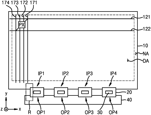
a display panel including a first input pad region, a second input pad region, a third input pad region, and a fourth input pad region;
a printed circuit board including a first output pad region, a second output pad region, a third output pad region, and a fourth output pad region; and
a flexible circuit board including a first end connected to the display panel and a second end connected to the printed circuit board,
wherein the first output pad region includes a 1st-1st output pad group and a 1st-2nd output pad group, each of the 1st-1st output pad group and the 1st-2nd output pad group including a plurality of test pads, wherein one test pad of the 1st-1st output pad group is connected to one test pad of the 1st-2nd output pad group,
wherein the second output pad region includes a 2nd-1st output pad group and a 2nd-2nd output pad group, each of the 2nd-1st output pad group and the 2nd-2nd output pad group including a plurality of test pads, wherein one test pad of the 2nd-1st output pad group is connected to one test pad of the 2nd-2nd output pad group,
wherein the third output pad region includes a 3rd-1st output pad group and a 3rd-2nd output pad group, each of the 3rd-1st output pad group and the 3rd-2nd output pad group including a plurality of test pads, wherein one test pad of the 3rd-1st output pad group is connected to one test pad of the 3rd-2nd output pad group,
wherein the fourth output pad region includes a 4th-1st output pad group and a 4th-2nd output pad group, each of the 4th-1st output pad group and the 4th-2nd output pad group including a plurality of test pads, wherein a test pad of the 4th-1st output pad group is connected to a test pad of the 4th-2nd output pad group, and
wherein the printed circuit board comprises:
a first input terminal electrically connected to the 1st-1st output pad group;
a second input terminal electrically connected to the 2nd-2nd output pad group;
a third input terminal electrically connected to the first input terminal; and
a fourth input terminal electrically connected to the 4th-2nd output pad group.
|