| CPC H01L 23/49555 (2013.01) [H01L 21/4825 (2013.01); H01L 21/4842 (2013.01); H01L 21/565 (2013.01); H01L 23/3107 (2013.01); H01L 23/4952 (2013.01); H01L 23/49537 (2013.01); H01L 23/49575 (2013.01); H01L 24/85 (2013.01); H01L 2224/8592 (2013.01); H01L 2924/1203 (2013.01); H01L 2924/14 (2013.01)] | 20 Claims |
|
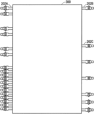
1. A manufacturing method of a semiconductor device, the method comprising:
providing at least one semiconductor element;
connecting, to the semiconductor element, a plurality of first terminals and at least one second terminal that is a control terminal to which a voltage lower than that of the first terminal is applied; and
forming a first bent part between a first portion and a second portion of the first terminal,
wherein on surfaces, facing each other, of the plurality of first terminals that are adjacent to each other, the first bent part does not protrude.
|