| CPC H01L 23/49537 (2013.01) [H01L 23/3114 (2013.01); H01L 23/4952 (2013.01); H01L 23/49513 (2013.01); H01L 23/49541 (2013.01); H01L 23/49562 (2013.01); H01L 23/49568 (2013.01); H01L 23/49575 (2013.01); H01L 24/49 (2013.01); H01L 2924/181 (2013.01)] | 21 Claims |
|
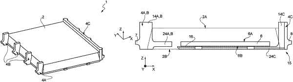
1. A device, comprising:
a molding compound including a first sidewall and a surface transverse to the first sidewall;
a first lead including a die attach portion and a lead portion coupled to the die attach portion, the lead portion extends outward from the first sidewall of the molding compound and extends outward from the surface of the molding compound;
a die coupled to the die attach portion by an adhesive, the die including:
a first surface coupled to the adhesive;
a second surface opposite to the first surface;
a first contact at the second surface; and
a second contact at the second surface and spaced apart from the first contact;
a second lead spaced apart from the first lead;
a third lead spaced apart from the second lead;
a first bonding wire coupling the first contact to the second lead; and
a second bonding wire coupling the second contact to the third lead.
|