| CPC H01L 23/315 (2013.01) [H01L 23/4952 (2013.01)] | 17 Claims |
|
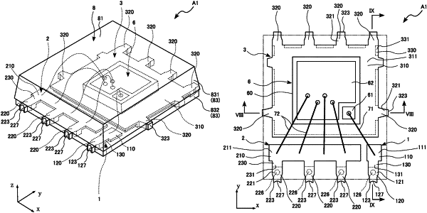
1. A semiconductor device comprising:
a semiconductor chip;
at least one lead electrically connected to the semiconductor chip;
a sealing resin that covers the semiconductor chip and a part of the lead, the sealing resin including a resin front surface and a resin back surface opposite to the resin front surface in a thickness direction; and
an island portion on which the semiconductor chip is mounted,
wherein the lead includes an end portion formed with a cut-out recessed inward in plan view, while also including a thin-walled portion that is smaller in thickness than a remaining portion of the lead,
wherein the lead includes an upper surface, the end portion of the lead includes a first lower surface, and the thin-walled portion of the lead includes a second lower surface, the second lower surface being offset toward the upper surface of the lead with respect to the first lower surface,
wherein the cut-out is at least partially round in plan view, and
wherein the sealing resin comprises a first resin side surface, a second resin side surface and a third resin side surface each of which is connected to the resin front surface and the resin back surface, and the island portion is formed with a plurality of protrusions each protruding outward from one of the first, second and third resin side surfaces in plan view.
|