| CPC H01L 22/32 (2013.01) [H01L 23/528 (2013.01); H01L 23/5226 (2013.01)] | 20 Claims |
|
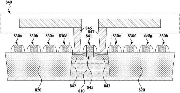
1. A semiconductor stress monitoring structure, comprising:
a substrate;
a plurality of first conductive segments over the substrate, arranged parallel to each other;
a plurality of second conductive segments arranged below the plurality of first conductive segments and parallel to each other, wherein the plurality of first conductive segments and the plurality of second conductive segments extend in the same direction; and
a sensing structure proximate to the substrate, configured to respond to a stress caused by the first conductive segments and the second conductive segments and generate a monitoring signal.
|