| CPC H01L 21/823857 (2013.01) [H01L 21/31105 (2013.01); H01L 21/823412 (2013.01); H01L 21/823431 (2013.01); H01L 21/823437 (2013.01); H01L 21/823462 (2013.01); H01L 21/823821 (2013.01); H01L 27/088 (2013.01); H01L 29/0665 (2013.01); H01L 29/42392 (2013.01); H01L 29/78696 (2013.01)] | 20 Claims |
|
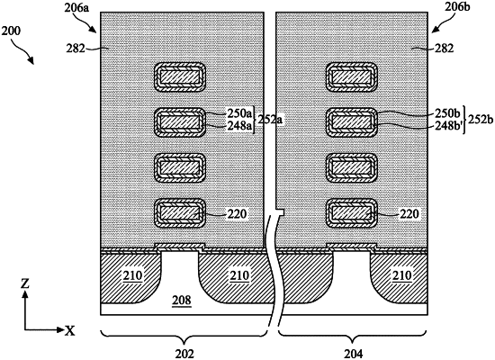
11. A method, comprising:
forming a plurality of first suspended layers in a first fin and a plurality of second suspended layers in a second fin;
forming a first interfacial layer wrapping around the first suspended layers in the first fin and a second interfacial layer wrapping around the second suspended layers in the second fin;
forming a first high-k dielectric layer wrapping around the first interfacial layer and a second high-k dielectric layer wrapping around the second interfacial layer;
depositing a metal layer wrapping around the first and second high-k dielectric layers;
removing the metal layer from the first high-k dielectric layer;
performing an annealing process, wherein during the annealing process, oxygen in an ambient environment is driven through the metal layer, the second high-k dielectric layer, and the second interfacial layer and arrives at an outer portion of the second suspended layers, such that the outer portion of the second suspended layers is converted to an oxide layer; and
depositing a first gate electrode layer wrapping around the first high-k dielectric layer and a second gate electrode layer wrapping around the second high-k dielectric layer.
|