| CPC H01L 21/823807 (2013.01) [H01L 21/02123 (2013.01); H01L 21/02236 (2013.01); H01L 21/02255 (2013.01); H01L 21/823821 (2013.01); H01L 21/823878 (2013.01); H01L 21/845 (2013.01); H01L 27/092 (2013.01); H01L 27/1207 (2013.01); H01L 27/1211 (2013.01); H01L 29/66545 (2013.01)] | 20 Claims |
|
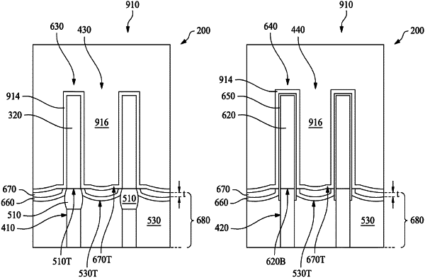
1. A device comprising:
a first fin structure disposed over a substrate, the first fin structure including:
a first semiconductor material layer; and
a second semiconductor material layer disposed on the first semiconductor layer; and
a first capping layer disposed directly on the first semiconductor material layer and the second semiconductor material layer of the first fin structure;
a second capping layer disposed directly on the first capping layer of the first fin structure, wherein the first and second capping layers have different material compositions, and wherein the first capping layer extends to a greater height above the substrate than the second capping layer;
a gate dielectric layer disposed on the first capping layer; and
a gate electrode layer disposed on the gate dielectric layer.
|