| CPC H01L 21/823418 (2013.01) [H01L 21/823462 (2013.01); H01L 21/823475 (2013.01); H01L 27/0617 (2013.01); H01L 29/0653 (2013.01); H01L 29/41725 (2013.01)] | 20 Claims |
|
1. A method of forming a semiconductor device, comprising:
providing a semiconductor substrate;
forming a first isolation structure and a second isolation structure for defining a first region and a second region in the semiconductor substrate;
performing a recessing process, such that the semiconductor substrate and the second isolation structure in the second region are recessed;
forming a first gate structure on the substrate in the first region, and a second gate structure on the substrate in the second region;
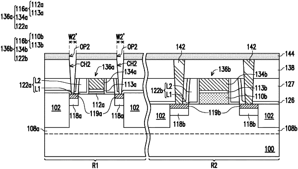
forming a first source/drain (S/D) region in the substrate within the first region and beside the first gate structure, and a second S/D region in the substrate within the second region and beside the second gate structure, wherein the first isolation structure is disposed laterally aside and in contact with the first S/D region within the first region, and the second isolation structure is disposed laterally aside and in contact with the second S/D region within the second region, wherein a top surface of the second isolation structure in the second region is lower than a top surface of the first isolation structure in the first region; and
forming a first S/D contact connected to the first S/D region and a second S/D contact connected to the second S/D region, wherein the first S/D contact and the second S/D contact are formed separately.
|