| CPC H01L 21/76897 (2013.01) [H01L 21/0228 (2013.01); H01L 21/0337 (2013.01); H01L 21/31144 (2013.01); H01L 21/76834 (2013.01); H01L 23/528 (2013.01); H01L 23/5226 (2013.01)] | 8 Claims |
|
1. A method of forming an interconnect structure, comprising:
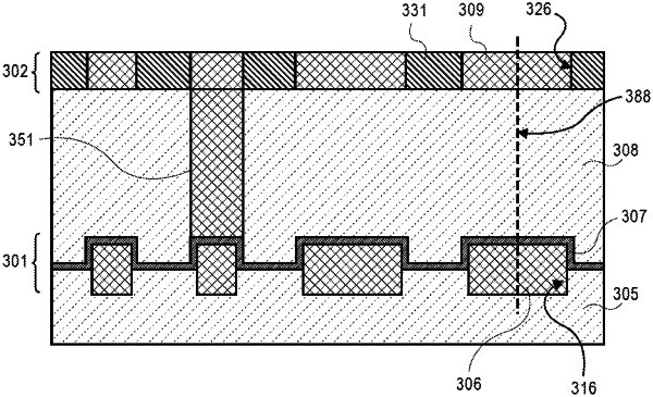
disposing a first interconnect layer in a first interlayer dielectric (ILD), wherein the first interconnect layer comprises a plurality of conductive traces;
recessing an uppermost surface of the first ILD, wherein the recessed uppermost surface of the first ILD is below uppermost surfaces of the first conductive traces;
disposing an etch stop layer over the first ILD and the first conductive traces;
selectively depositing a helmet layer over the first conductive traces, wherein the helmet layer is deposited with an atomic layer deposition (ALD) processes that comprises spinning a substrate on which the interconnect structure is formed;
disposing a second ILD over the interconnect structure, wherein the second ILD fills gaps between portions of the helmet layer on corresponding ones of the first conductive traces;
disposing a first hardmask layer over the second ILD;
removing the helmet layer; and
disposing a third ILD in the gaps between the second ILD.
|