| CPC H01L 21/76877 (2013.01) [H01L 21/76802 (2013.01); H01L 21/76832 (2013.01); H01L 23/528 (2013.01); H01L 23/53209 (2013.01)] | 20 Claims |
|
1. A method for fabricating an integrated circuit device, comprising:
forming a first conductive feature in a first portion of a first interlayer dielectric layer, and a second conductive feature in a second portion of the first interlayer dielectric layer;
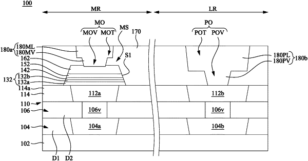
forming a memory structure over and in contact with the first conductive feature, wherein the memory structure comprises at least a resistance switching element over the first conductive feature;
forming a third conductive feature over and in contact with second conductive feature, wherein a top surface of the third conductive feature is higher than a top surface of the memory structure, the third conductive feature comprises a first conductive line, and the first conductive line of the third conductive feature has a bottom surface lower than the top surface of the memory structure and higher than a bottom surface of the memory structure, a top surface higher than the top surface of the memory structure, and a substantially straight sidewall extending from the bottom surface of the first conductive line to the top surface of the first conductive line; and
forming a fourth conductive feature over and in contact with the memory structure, wherein the fourth conductive feature comprises a second conductive line, the top surface of the first conductive line is substantially level with a top surface of the second conductive line, and the bottom surface of the first conductive line is lower than a bottommost portion of a bottom surface of the second conductive line.
|