US 11,894,266 B2
Metal capping layer and methods thereof
Shao-Kuan Lee, Kaohsiung (TW); Cheng-Chin Lee, Taipei (TW); Hsin-Yen Huang, New Taipei (TW); Hai-Ching Chen, Hsinchu (TW); and Shau-Lin Shue, Hsinchu (TW)
Assigned to TAIWAN SEMICONDUCTORMANUFACTURING CO., LTD., Hsinchu (TW)
Filed by Taiwan Semiconductor Manufacturing Co., Ltd., Hsin-Chu (TW)
Filed on Dec. 12, 2022, as Appl. No. 18/064,561.
Application 18/064,561 is a continuation of application No. 17/443,506, filed on Jul. 27, 2021, granted, now 11,527,435.
Application 17/443,506 is a continuation of application No. 16/270,057, filed on Feb. 7, 2019, granted, now 11,075,113, issued on Jul. 27, 2021.
Claims priority of provisional application 62/692,436, filed on Jun. 29, 2018.
Prior Publication US 2023/0112282 A1, Apr. 13, 2023
Int. Cl. H01L 21/76 (2006.01); H01L 21/32 (2006.01); H01L 21/768 (2006.01); H01L 23/528 (2006.01); H01L 23/522 (2006.01); H01L 23/532 (2006.01); H01L 21/02 (2006.01); H01L 21/285 (2006.01); H01L 21/321 (2006.01)
CPC H01L 21/7685 (2013.01) [H01L 21/02118 (2013.01); H01L 21/28568 (2013.01); H01L 21/76828 (2013.01); H01L 21/76834 (2013.01); H01L 21/76843 (2013.01); H01L 21/76877 (2013.01); H01L 23/528 (2013.01); H01L 23/5226 (2013.01); H01L 23/53209 (2013.01); H01L 23/53238 (2013.01); H01L 21/3212 (2013.01); H01L 21/7684 (2013.01); H01L 23/53266 (2013.01)] 20 Claims
OG exemplary drawing
 
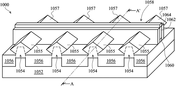
1. A method, comprising:
forming a dielectric layer over a substrate;
forming a metal layer embedded within the dielectric layer;
selectively depositing a capping layer on the metal layer without depositing on the dielectric layer;
forming a self-assembled monolayer (SAM) over the capping layer, the SAM having a first portion and a second portion materially different from the first portion; and
removing the second portion of the SAM while the first portion of the SAM remains on the capping layer.