| CPC H01L 21/76254 (2013.01) [H01L 21/02164 (2013.01); H01L 21/02274 (2013.01); H01L 27/1203 (2013.01)] | 14 Claims |
|
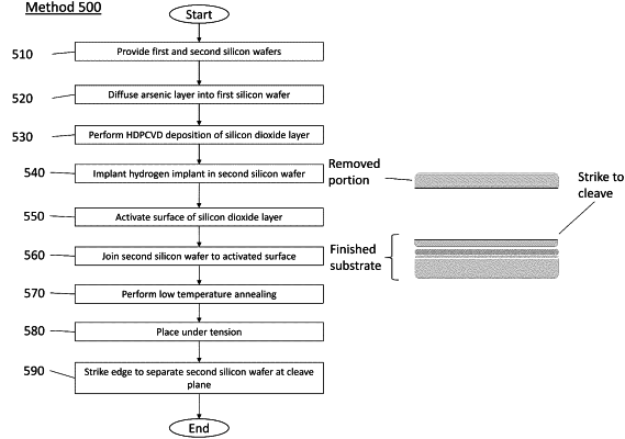
1. A method, comprising:
providing a first silicon wafer having a first side and a second side;
diffusing arsenic into the first side of the first silicon wafer so as to produce a diffused arsenic layer,
wherein the diffused arsenic layer has a first side and a second side opposite the first side of the diffused arsenic layer,
wherein the diffused arsenic layer is positioned within the first silicon wafer such that the first side of the diffused arsenic layer is positioned between the first and second sides of the first silicon wafer, and such that the second side of the diffused arsenic layer is positioned at the second side of the first silicon wafer,
wherein a thickness of the diffused arsenic layer is in a range of from 1 micron to 10 microns, and
wherein the entire diffused arsenic layer has a trap density that is in a range of 0.8*1010 cm2 eV−1 to 1.2*1010 cm2 eV−1;
depositing a silicon dioxide layer on the first side of the first silicon wafer using a high density plasma chemical vapor deposition (HDPCVD) process,
wherein the HDPCVD process uses an inductively-coupled plasma source,
wherein the inductively-coupled plasma source is operated at a power that is in a range of from 65 watts to 225 watts,
wherein the HDPCVD process uses a flow of oxygen gas, a flow of silane gas, and a flow of argon gas,
wherein a flow rate of the flow of oxygen gas is in a range of from 20 to 35 sccm,
wherein a flow rate of the flow of silane gas is in a range of 20 to 35 sccm, and
wherein a flow rate of the flow of argon gas in a range of from 20 to 35 sccm,
wherein the HDPCVD process is performed at a pressure that is in a range of from 5 millitorr to 20 millitorr,
wherein the HDPCVD process is performed using a bias power that is in a range of from 0 to 100 watts,
wherein the HDPCVD process is performed with the first silicon wafer held at a temperature that is in a range of from 100 to 250 degrees Celsius,
wherein a deposition rate of the silicon dioxide layer is in a range of from 900 to 1100 angstroms per minute, and
wherein a thickness of the silicon dioxide layer is in a range of from 1500 to 5000 angstroms;
providing a second silicon wafer having a first side and a second side opposite the first side of the second silicon wafer;
introducing a hydrogen implant into the second silicon wafer so as to define a cleave plane,
wherein a thickness of a portion of the second silicon wafer between the first side of the second silicon wafer and the cleave plane is in a range of from 500 to 5000 angstroms;
activating the silicon dioxide layer,
wherein the activating step comprises low-pressure plasma-activated bonding at a pressure in a range of from 0.1 to 100 Pa;
contacting the first side of the second silicon wafer to the activated silicon dioxide layer, thereby producing a combined wafer;
annealing the combined wafer,
wherein the annealing is performed at a temperature in a range of from 200 to 400 degrees Celsius for a duration in a range of from one hour to eight hours;
applying a tension to the combined wafer in a direction so as to urge the first silicon wafer and the second silicon wafer apart from one another; and
striking an edge of the second silicon wafer so as to cleave the second silicon wafer at the cleave plane, thereby producing a silicon-on-insulator substrate.
|