| CPC H01L 21/76224 (2013.01) [H01L 21/764 (2013.01); H01L 21/823437 (2013.01); H01L 21/823481 (2013.01); H01L 27/0886 (2013.01)] | 20 Claims |
|
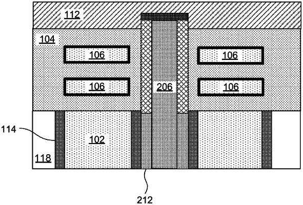
1. A semiconductor structure comprising:
a substrate;
a gate structure over the substrate; and
a cut feature between two separate portions of the gate structure and in direct contact with both the two separate portions of the gate structure,
wherein the cut feature comprises a dielectric layer and a work-function layer between the dielectric layer and the two separate portions of the gate structure, and
wherein the work-function layer directly contacts the dielectric layer and is spaced apart from a channel region surrounded by the gate structure.
|