| CPC H01L 21/76224 (2013.01) [H01L 21/768 (2013.01); H01L 21/76816 (2013.01); H01L 21/76831 (2013.01); H01L 21/76834 (2013.01); H01L 21/76897 (2013.01)] | 20 Claims |
|
1. A method of manufacturing a semiconductor device structure, comprising:
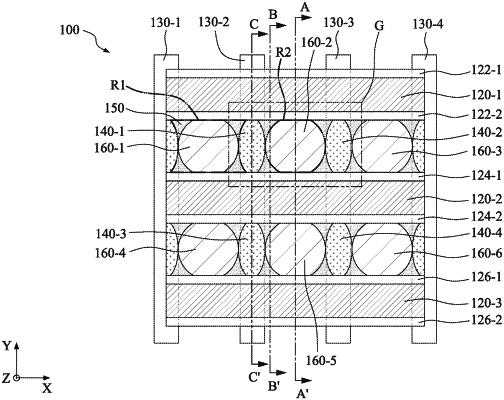
forming a first metallization line and a second metallization line extending in a parallel;
forming a first isolation feature and a second isolation feature between the first metallization line and the second metallization line and perpendicularly extended between the first metallization line and the second metallization line, wherein the first metallization line, the second metallization line, the first isolation feature and the second isolation feature define an aperture and form a boundary of the aperture;
forming a profile modifier within the aperture, wherein the profile modifier comprises a plurality of segments spaced apart from each other, wherein each of the segments are located at corners of the aperture; and
forming a contact feature surrounded by the plurality of segments.
|