| CPC H01L 21/568 (2013.01) [H01L 23/49816 (2013.01); H01L 24/19 (2013.01); H01L 2224/04105 (2013.01); H01L 2224/12105 (2013.01); H01L 2224/73267 (2013.01)] | 11 Claims |
|
1. A method for manufacturing a wafer system-level fan-out packaging structure, comprising:
providing a first carrier substrate and a release layer on the first carrier substrate;
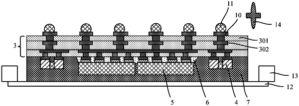
forming a redistribution layer, wherein the redistribution layer comprises a first surface and a second surface opposite to each other, wherein the first surface of the redistribution layer is placed on the release layer;
bonding a patch element to the second surface of the redistribution layer;
providing a die having a bump disposed on a front side, and bonding the front side of the die to the second surface of the redistribution layer by the bump;
forming a plastic packaging layer on the second surface of the redistribution layer, wherein the plastic packaging layer covers the patch element, a back side and side surfaces of the die;
forming a second carrier substrate, wherein the second carrier substrate is bonded to the plastic packaging layer;
bonding the second carrier substrate to the plastic packaging layer; and
removing the first carrier substrate and the release layer to expose the first surface of the redistribution layer;
forming a solder bump on the first surface of the redistribution layer; and
removing the second carrier substrate.
|