| CPC H01L 21/565 (2013.01) [H01L 23/24 (2013.01); H01L 21/561 (2013.01); H01L 24/16 (2013.01); H01L 24/48 (2013.01); H01L 24/73 (2013.01); H01L 2224/16227 (2013.01); H01L 2224/48227 (2013.01); H01L 2224/73204 (2013.01); H01L 2224/73265 (2013.01)] | 20 Claims |
|
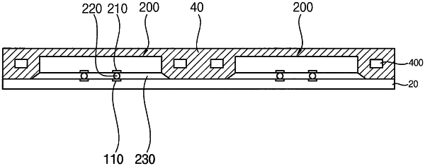
1. A method of manufacturing a semiconductor package, the method comprising:
disposing a semiconductor chip on a substrate;
disposing the substrate in a cavity between a lower mold and an upper mold of a molding apparatus;
after disposing the substrate in the cavity, a mechanical reinforcing pattern around the semiconductor chip within the cavity such that the mechanical reinforcing pattern is suspended at a predetermined height from the substrate;
injecting a molding material into the cavity; and
curing the molding material within the cavity.
|