| CPC H01L 21/4857 (2013.01) [H01L 21/486 (2013.01); H01L 21/4853 (2013.01); H01L 23/49816 (2013.01); H01L 23/49822 (2013.01); H01L 23/49838 (2013.01); H01L 23/5226 (2013.01); H01L 23/5383 (2013.01); H01L 24/80 (2013.01); H01L 2224/80345 (2013.01); H01L 2224/80355 (2013.01)] | 20 Claims |
|
1. A method comprising:
forming a first package component comprising:
forming a first plurality of openings in a first dielectric layer;
depositing a first metallic material into the first plurality of openings;
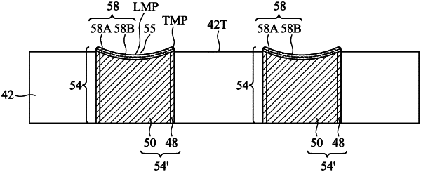
performing a planarization process on the first metallic material and the first dielectric layer to form a first plurality of metal pads in the first dielectric layer, wherein one of the first plurality of metal pads comprises edge portions and a middle portion more recessed than the respective edge portions; and
selectively depositing a second metallic material over the first plurality of metal pads to form a first plurality of bond pads, wherein the first plurality of bond pads comprise the first plurality of metal pads and corresponding parts of the second metallic material; and
bonding the first package component to a second package component, wherein before the bonding, the first dielectric layer comprises a first top surface, and the second metallic material comprises a second top surface, and wherein the second top surface comprises a first point lower than the first top surface, and a second point higher than the first top surface, and wherein the first plurality of bond pads are bonded to the second package component.
|