US 11,894,240 B2
Semiconductor processing systems with in-situ electrical bias
David Hurley, Dublin (IE); Ioan Domsa, Dublin (IE); Ian Colgan, Dublin (IE); Gerhardus Van Der Linde, Dublin (IE); Patrick Hughes, Dublin (IE); Maciej Burel, Dublin (IE); Barry Clarke, Dublin (IE); Mihaela Ioana Popovici, Leuven (BE); Lars-Ake Ragnarsson, Leuven (BE); Gerrit J. Leusink, Albany, NY (US); Robert Clark, Fremont, CA (US); and Dina Triyoso, Albany, NY (US)
Assigned to TOKYO ELECTRON LIMITED, Tokyo (JP)
Filed by Tokyo Electron Limited, Tokyo (JP)
Filed on Feb. 25, 2021, as Appl. No. 17/185,231.
Application 17/185,231 is a continuation in part of application No. 16/841,342, filed on Apr. 6, 2020, granted, now 11,335,792.
Prior Publication US 2021/0313189 A1, Oct. 7, 2021
Int. Cl. H01L 21/326 (2006.01); H01L 21/04 (2006.01); H01L 21/42 (2006.01); H01L 21/02 (2006.01)
CPC H01L 21/326 (2013.01) [H01L 21/02107 (2013.01); H01L 21/0425 (2013.01); H01L 21/42 (2013.01)] 23 Claims
OG exemplary drawing
 
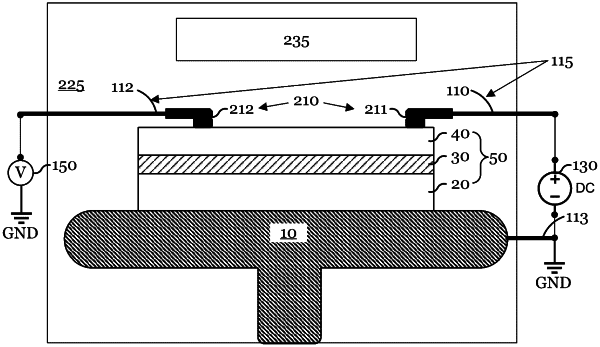
1. A system for processing semiconductor wafers, the system comprising:
a processing chamber;
a heat source;
a substrate holder configured to expose a semiconductor wafer to the heat source;
a first electrode configured to be detachably attached to the semiconductor wafer, a conductive outer surface of the first electrode configured to be in physical contact with a first major surface of the semiconductor wafer when the first electrode is attached detachably to the semiconductor wafer; and
a second electrode coupled to the substrate holder, the first electrode and the second electrode together configured to apply an electric field in the semiconductor wafer.