| CPC H01L 21/3088 (2013.01) [H01L 21/3086 (2013.01); H01L 21/32139 (2013.01); H01L 21/823431 (2013.01); H01L 21/823437 (2013.01)] | 20 Claims |
|
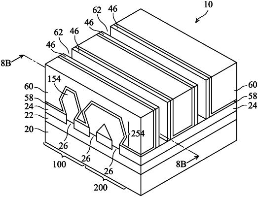
1. A method comprising:
forming a first mask layer over a target layer;
forming a second mask layer over the first mask layer, wherein the second mask layer is patterned with an opening therein to reveal a first portion of the first mask layer, and wherein a second portion of the first mask layer is covered by the second mask layer;
depositing a third mask layer comprising:
a first part over the second mask layer; and
a second part extending into the opening to contact the first mask layer;
etching the third mask layer and the first mask layer, wherein after the etching, the first mask layer comprises:
a remaining portion of the first portion, wherein portions of the first mask layer on opposite sides of the remaining portion are removed; and
transferring patterns of the first mask layer into the target layer.
|