| CPC H01L 21/3086 (2013.01) [H01L 21/0228 (2013.01); H01L 21/0273 (2013.01); H10B 12/03 (2023.02); H10B 12/30 (2023.02)] | 15 Claims |
|
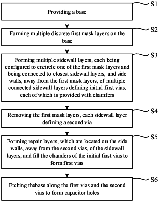
1. A method for manufacturing a semiconductor structure, comprising:
providing a base;
forming multiple discrete first mask layers on the base;
forming multiple sidewall layers, wherein each sidewall layer is configured to encircle one of the first mask layers, each sidewall layer is connected to closest sidewall layers, side walls, away from the first mask layers, of the multiple connected sidewall layers define initial first vias, and each of the initial first vias is provided with chamfers;
removing the first mask layers, wherein each sidewall layer defines a second via;
forming repair layers, after removing the first mask layers, wherein the repair layers are located on side walls, away from the second vias, of the sidewall layers; and the repair layers fill the chamfers of the initial first vias to form first vias; and
etching the base along the first vias and the second vias to form capacitor holes located in the base.
|