| CPC H01L 21/302 (2013.01) [H01L 21/48 (2013.01); H01L 21/561 (2013.01); H01L 21/565 (2013.01); H01L 21/78 (2013.01); H01L 23/12 (2013.01); H01L 23/3185 (2013.01); H01L 24/04 (2013.01); H01L 24/26 (2013.01); H01L 2224/94 (2013.01)] | 18 Claims |
|
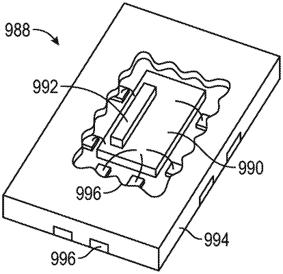
1. A semiconductor device comprising:
a semiconductor die comprising a first largest planar surface, a second largest planar surface and a thickness between the first largest planar surface and the second largest planar surface; and
a temporary die support structure coupled to one of the first largest planar surface or the second largest planar surface;
wherein the semiconductor die is coupled with one of a substrate, a leadframe, an interposer, a package, a bonding surface, or a mounting surface;
wherein a perimeter of the temporary die support structure is less than and within a perimeter of the semiconductor die; and
wherein the thickness is between 0.1 microns and 125 microns.
|