| CPC H01L 21/0338 (2013.01) [H01L 21/0332 (2013.01); H01L 21/0335 (2013.01); H01L 21/0337 (2013.01)] | 14 Claims |
|
1. A method for forming a semiconductor structure, comprising:
providing a to-be-etched layer;
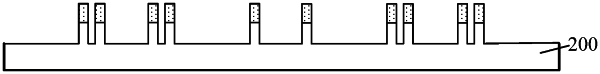
forming a plurality of core layers on the to-be-etched layer, wherein a first opening and a second opening are formed between different adjacent core layers, and a width of the first opening is smaller than a width of the second opening;
forming a first sacrificial material layer on the to-be-etched layer and the plurality of core layers, the first sacrificial material layer being formed on a top surface and sidewall surfaces of the first opening and the second opening and on top surfaces of the plurality of core layers;
forming an initial second sacrificial layer on a top surface and sidewall surfaces of the first sacrificial material layer in the first opening to fully fill the first opening and on sidewall surfaces of the first sacrificial material layer in the second opening, the initial second sacrificial layer being formed after the first sacrificial material layer is formed without removing a portion of the first sacrificial material layer;
after the initial second sacrificial layer is formed, removing a portion of the initial second sacrificial layer on the sidewall surfaces of the first sacrificial material layer in the second opening to form a second sacrificial layer on the top surface and the sidewall surfaces of the first sacrificial material layer in the first opening only and fully filing the first opening;
after forming the second sacrificial layer, removing a portion of the first sacrificial material layer on the top surfaces of the plurality of core layers to form an initial first sacrificial layer;
removing the plurality of core layers after forming the initial first sacrificial layer and the second sacrificial layer;
modifying the initial first sacrificial layer to form a first sacrificial layer;
forming sidewall spacers on sidewall surfaces of the first sacrificial layer after removing the plurality of core layers;
after forming the sidewall spacers, removing the second sacrificial layer;
after removing the second sacrificial layer, removing the first sacrificial layer, a material of the second sacrificial layer being different from a material of the first sacrificial layer; and
after removing the first sacrificial layer, forming a semiconductor structure by etching the to-be etched layer using the sidewall spacers as a mask.
|