| CPC H01L 21/0332 (2013.01) [H01L 21/0337 (2013.01); H10B 41/27 (2023.02); H01L 21/31122 (2013.01); H01L 21/31144 (2013.01)] | 6 Claims |
|
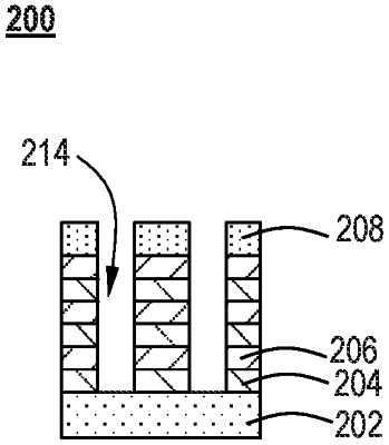
1. A memory device comprising:
a memory stack comprising a plurality of alternating layers of a first material and a second material on a substrate;
a first nanocrystalline diamond layer on the memory stack, the first nanocrystalline diamond layer having a first thickness, a first roughness of greater than about 25 nm, a first hardness, an sp3 content of greater than 80%, and a crystal size in a range of from 2 nm to 5 nm;
a second nanocrystalline diamond layer on the first nanocrystalline diamond layer, the second nanocrystalline diamond layer having a second thickness, an sp3 content of greater than 80%, a crystal size in a range of from 2 nm to 5 nm, and a second roughness of less than about 15 nm; and
a memory channel extending from a top surface of the memory stack to the substrate.
|