| CPC H01L 21/02118 (2013.01) [H01L 21/02002 (2013.01); H01L 21/0274 (2013.01); H01L 21/02345 (2013.01)] | 8 Claims |
|
1. A method for manufacturing a semiconductor device, comprising:
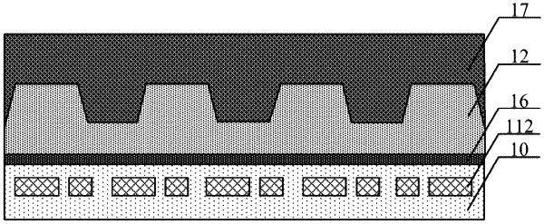
providing a substrate, wherein the substrate is divided into a plurality of chip areas by scribe lines, wherein the scribe lines comprise test pads;
forming a protective layer on the substrate, wherein the protective layer comprises a first portion and a second portion, wherein the first portion covers the plurality of chip areas, wherein the second portion covers the scribe lines;
performing a first lithography with a first photomask to expose and develop the first portion of the protective layer to form a plurality of grooves, wherein a depth of each of the plurality of grooves is less than an initial thickness of the protective layer;
performing a second lithography with a second photomask to expose and develop the second portion of the protective layer to form test pads; and
performing a third lithography with a third photomask to further expose and develop the first portion of the protective layer for the plurality of chip areas and the second portion of the protective layer for test pads.
|