| CPC H01J 37/32082 (2013.01) [H01J 37/32926 (2013.01); H01L 21/31116 (2013.01); H01J 2237/334 (2013.01)] | 20 Claims |
|
1. A method of reducing reflected Radio Frequency (RF) power in substrate processing chambers, the method comprising:
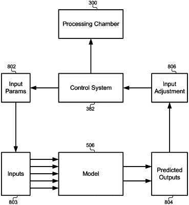
accessing a plurality of input parameters for a processing chamber, wherein the plurality of input parameters are in part derived from a recipe for the processing chamber to perform a process on a substrate;
providing the plurality of input parameters for the processing chamber to a model, wherein the model has been trained using previous pluralities of input parameters and corresponding pluralities of sensor measurements;
receiving one or more first outputs from the model that indicate a predicted first amount of RF power that will be reflected back from the processing chamber to an RF source when igniting a plasma in the processing chamber; and
adjusting the plurality of input parameters based on the predicted first amount of RF power that is reflected back from the processing chamber.
|