| CPC H01G 4/30 (2013.01) [H01G 4/008 (2013.01); H01G 4/012 (2013.01); H01G 4/12 (2013.01); H01G 4/224 (2013.01)] | 23 Claims |
|
1. A multilayer ceramic capacitor comprising:
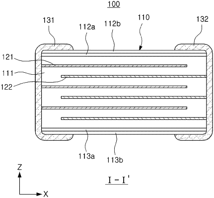
a ceramic body including a dielectric layer, and a first internal electrode and a second internal electrode, disposed to oppose each other with the dielectric layer interposed therebetween, and including a first surface and a second surface, opposing each other in a first direction, a third surface and a fourth surface, opposing each other in a second direction, and a fifth surface and a sixth surface, opposing each other in a third direction; and
a first external electrode disposed on the first surface of the ceramic body and connected to the first internal electrode, and a second external electrode disposed on the second surface of the ceramic body and connected to the second internal electrode,
wherein the ceramic body further comprises:
a capacitance formation portion including the first internal electrode and the second internal electrode, stacked in the third direction with the dielectric layer interposed therebetween, to form capacitance;
a first margin portion and a second margin portion disposed on both surfaces of the capacitance formation portion, respectively, in the second direction; and
a first cover portion and a second cover portion, disposed on both surfaces of the capacitance formation portion, both surfaces of the first margin portion, and both surfaces of the second margin portion in the third direction, respectively,
wherein the first and second cover portions each comprise a first cover layer adjacent to an internal electrode, disposed on an outermost side among the first and second internal electrodes, and immediately adjacent to the capacitance formation portion, and a second cover layer disposed on the first cover layer, and an interface at which the first cover layer and the second cover layer are in contact with each other, and
wherein an average density of the second cover layer is higher than an average density of the first cover layer.
|