| CPC H01G 4/2325 (2013.01) [H01B 1/22 (2013.01); H01F 17/0013 (2013.01); H01F 27/29 (2013.01); H01F 27/292 (2013.01); H01F 27/32 (2013.01); H01F 27/324 (2013.01); H01G 4/232 (2013.01); H01G 4/252 (2013.01); H01G 4/30 (2013.01); H01G 13/006 (2013.01); H03H 7/427 (2013.01); H05K 1/0306 (2013.01); H01F 2017/0066 (2013.01); H01F 2017/0093 (2013.01); H01G 4/12 (2013.01); H03H 2001/0057 (2013.01); H03H 2001/0085 (2013.01); H05K 3/3442 (2013.01); H05K 2201/1006 (2013.01); H05K 2201/10636 (2013.01)] | 9 Claims |
|
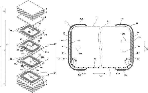
1. An electronic component comprising:
an element body including a principal surface including a ceramic material and a side surface adjacent to the principal surface, the principal surface being arranged to constitute a mounting surface;
an external electrode including a first electrode portion disposed on the principal surface and a second electrode portion disposed on the side surface;
a resin film disposed on the principal surface and in contact with the principal surface, and having electrical insulating properties; and
an internal conductor disposed in the element body and including an end exposed at the side surface,
wherein each of the first electrode portion and the second electrode portion includes a conductive resin layer disposed on the element body,
the conductive resin layer included in the first electrode portion is disposed on the resin film and is in contact with the resin film,
the second electrode portion includes a sintered metal layer connected with the end of the internal conductor, the sintered metal layer is disposed on the side surface and is in contact with the side surface,
the conductive resin layer included in the second electrode portion is disposed on the element body in such a manner that the sintered metal layer is disposed between the element body and the conductive resin layer included in the second electrode portion,
the resin film includes an end portion covering an edge of the sintered metal layer, and
the end portion of the resin film is located between the edge of the sintered metal layer and the conductive resin layer and is in direct contact with the edge of the sintered metal layer and the conductive resin layer.
|