| CPC H01G 4/1227 (2013.01) [H01G 4/30 (2013.01); H01G 4/012 (2013.01); H01G 4/232 (2013.01)] | 26 Claims |
|
1. A multilayer electronic component, comprising:
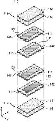
a body including a plurality of first dielectric layers, an active portion in which internal electrodes are alternately disposed, and a cover portion disposed on the active portion in a first direction of the body, a direction in which the plurality of first dielectric layers are laminated, the cover portion including a second dielectric layer; and
an external electrode disposed externally on the body and connected to one of the internal electrodes,
wherein the body includes a margin portion covering all side surfaces of the one of the internal electrodes other than a side surface connected to the external electrode, and
wherein the margin portion includes a dielectric pattern having a porosity higher than that of one of the plurality of first dielectric layers.
|