| CPC H01G 4/1227 (2013.01) [C04B 35/4682 (2013.01); H01G 4/30 (2013.01); H01G 4/008 (2013.01)] | 29 Claims |
|
1. A multilayer ceramic electronic component, comprising:
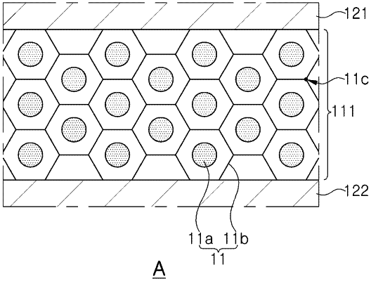
a ceramic body including a dielectric layer having a main component represented by (Ba1-xCax)(Ti1-y(Zr, Sn, Hf)y)O3 (where, 0≤x≤1, 0≤y≤0.5), and having a plurality of grains and grain boundaries disposed between the plurality of grains, and including first and second internal electrodes alternately stacked with the dielectric layer interposed therebetween;
a first external electrode connected to the first internal electrode; and
a second external electrode connected to the second internal electrode,
wherein the dielectric layer comprises a triple point disposed in contact with three grain boundaries and a secondary phase of Si disposed inside the triple point,
wherein a dispersion of an Si content at an interface between the dielectric layer and the internal electrode is 1% by weight or less.
|