| CPC H01G 4/012 (2013.01) [H01G 4/1227 (2013.01); H01G 4/232 (2013.01); H01G 4/30 (2013.01)] | 20 Claims |
|
1. A multilayer electronic component comprising:
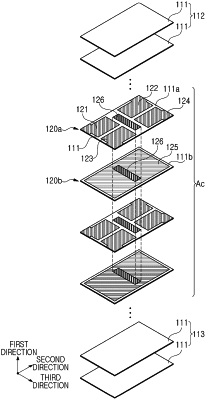
a first internal electrode layer including a first dielectric layer and first to fourth internal electrodes disposed to be spaced apart from each other on the first dielectric layer;
a second internal electrode layer including a second dielectric layer and a fifth internal electrode disposed on the second dielectric layer;
a body including a capacitance forming portion in which the first internal electrode layer and the second internal electrode layer are alternately disposed;
a connection electrode penetrating through the first and second internal electrode layers, spaced apart from the first to fourth internal electrodes, and connected to the fifth internal electrode;
first to fourth external electrodes disposed to be connected to the first to fourth internal electrodes, respectively, on the body; and
a fifth external electrode disposed to be connected to the connection electrode on the body.
|