| CPC G11C 7/222 (2013.01) [H01L 25/0657 (2013.01); H01L 25/18 (2013.01); H03K 3/017 (2013.01); H01L 2225/06541 (2013.01)] | 23 Claims |
|
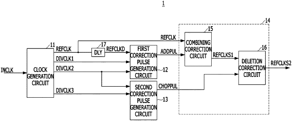
1. A duty correction device, comprising:
a clock generation circuit configured to generate first to third divided clock signals, each having a phase offset from a reference clock signal;
a first correction pulse generation circuit configured to generate a first correction pulse by detecting a phase difference between a delayed clock signal and the first and second divided clock signals, the delayed clock signal generated by delaying the reference clock signal;
a second correction pulse generation circuit configured to generate a second correction pulse by detecting a phase difference between the second and third divided clock signals; and
a duty correction circuit configured to check whether the first and second correction pulses are generated at a preset logic level of the reference clock signal, and to reflect at least one of the first or second correction pulses in a duty correction operation for the reference clock signal according to a result of the check.
|