| CPC G11C 7/065 (2013.01) [G11C 7/106 (2013.01); G11C 7/109 (2013.01); G11C 7/1063 (2013.01); G11C 7/1087 (2013.01)] | 20 Claims |
|
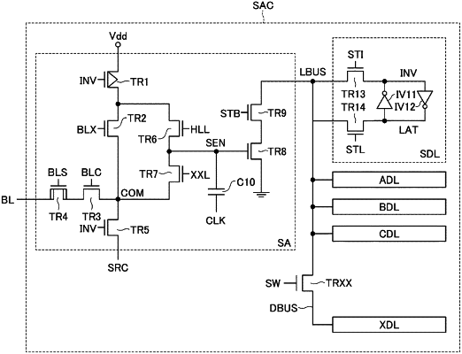
1. A semiconductor memory device comprising:
a plurality of data latch circuits that are used for input and output of data between a sense amplifier circuit and an input/output circuit; and
a data wiring that is connected to the plurality of data latch circuits, wherein
each of the data latch circuits includes
a data storage unit that temporarily stores data input and output between the sense amplifier circuit and the input/output circuit, and
at least two N-channel type MOS transistors and at least one P-channel type MOS transistor provided between the data storage unit and the data wiring, and
a common signal line is connected to gates of the at least two N-channel type MOS transistors.
|