| CPC G11C 29/42 (2013.01) [G11C 29/026 (2013.01); G11C 29/10 (2013.01); G11C 29/4401 (2013.01); G11C 2029/1204 (2013.01)] | 18 Claims |
|
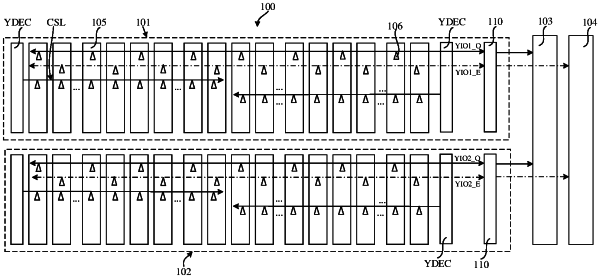
1. A memory, comprising banks, each of the banks comprising a U half bank and a V half bank;
a first error checking and correcting unit connected with U half banks and V half banks and configured to check and correct errors of output data of the U half banks and the V half banks; and
a second error checking and correcting unit connected with the U half banks and the V half banks and configured to check and correct errors of output data of the U half banks and the V half banks;
wherein each of the U half banks comprises an even number of block data buses, and the block data buses are sequentially numbered from zero according to natural numbers;
wherein odd-numbered block data buses are connected with the first error checking and correcting unit, and even-numbered block data buses are connected with the second error checking and correcting unit; or the odd-numbered block data buses are connected with the second error checking and correcting unit, and the even-numbered block data buses are connected with the first error checking and correcting unit.
|