| CPC G11C 29/38 (2013.01) [G11C 29/18 (2013.01)] | 20 Claims |

|
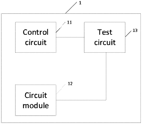
1. A test circuit comprising:
an input terminal, a processing circuit and an output terminal;
wherein the input terminal receives an input signal, wherein the input signal comprises a test command to instruct a test target circuit module and an address of a target circuit module;
wherein the processing circuit is configured to determine a test mode signal according to the test command and the address of the target circuit module, wherein the test mode signal carries a test type, wherein the test mode signal triggers the target circuit module to perform a test according to the test type; and
wherein the output terminal sends the test mode signal to the target circuit module according to the address of the target circuit module;
wherein the processing circuit comprises:
a first address latch, a second address latch, a command logic circuit, a control logic circuit, a test decoding circuit and a slave latch;
wherein the first address latch receives a first internal address and outputs a first internal delay address;
wherein the command logic circuit receives the test command and a second internal address, and outputs a test mode command; and
wherein the second address latch receives a third internal address and the test mode command, and outputs a third internal delay address;
wherein the control logic circuit is configured to receive the first internal delay address and the test mode command, and outputs a test mode enable active signal and a test mode enable slave signal;
wherein the test decoding circuit is configured to receive the first internal delay address and the third internal delay address, and outputs a decoding signal; and
wherein the slave latch receives the third internal address and the test mode enable slave signal, and outputs a slave address.
|