| CPC G11C 29/1201 (2013.01) [G11C 29/12015 (2013.01); G11C 29/36 (2013.01); G11C 29/46 (2013.01); G11C 2029/3602 (2013.01)] | 20 Claims |
|
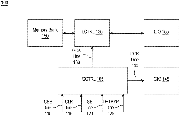
1. A memory device, comprising:
a plurality of memory cells arranged in an array;
an input/output (I/O) interface, connected to the plurality of memory cells to output data signal from each memory cell; and
a control circuit, comprising:
a first clock generator configured to generate a first clock signal and a second clock signal according to an input clock signal and a chip enable (CE) signal, and provide the first clock signal to the plurality of memory cells; and
a second clock generator distinct from the first clock generator, and configured to generate a third clock signal according to the input clock signal and provide the first clock generator with a design for testability (DFT) enable (DFTEN) signal;
wherein the control circuit generates an output clock signal according to the second clock signal or the third clock signal.
|