| CPC G11C 16/26 (2013.01) [G11C 16/08 (2013.01); G11C 16/10 (2013.01); G11C 16/24 (2013.01); G11C 16/30 (2013.01); H10B 43/27 (2023.02); H10B 43/30 (2023.02)] | 20 Claims |

|
1. A semiconductor memory device comprising:
first and second memory cells;
a first word line connected to the first memory cell;
a second word line connected to the second memory cell;
a first bit line connected to the first memory cell;
a second bit line connected to the second memory cell;
a first sense amplifier connected to the first bit line, the first sense amplifier having a first node to determine data;
a second sense amplifier connected to the second bit line, the second sense amplifier having a second node to determine data; and
a control circuit which supplies control signals to the first sense amplifier and the second sense amplifier,
wherein in a read operation,
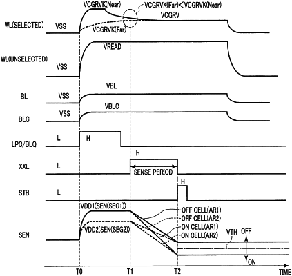
the control circuit supplies a first control signal to connect the first node of the first sense amplifier to the first bit line, and a second control signal to connect the second node of the second sense amplifier to the second bit line, and
a timing at which supply of the first control signal ends and a timing at which supply of the second control signal ends are different.
|