| CPC G11C 16/26 (2013.01) [G11C 16/0433 (2013.01); G11C 16/08 (2013.01); G11C 16/102 (2013.01); G11C 16/24 (2013.01); G11C 16/30 (2013.01)] | 20 Claims |
|
1. A memory device comprising:
an unselected sub-block comprising:
a bit line;
a drain select (SGD) transistor coupled with the bit line;
a source voltage line;
a source select (SGS) transistor coupled with the source voltage line; and
a plurality of wordlines coupled with gates of a string of memory cells, wherein the string of memory cells comprises a channel coupled between the SGS transistor and SGD transistor; and
control logic operatively coupled with the unselected sub-block, the control logic to perform operations comprising:
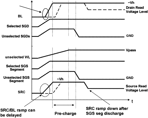
causing the SGD and SGS transistors to be turned on while ramping the plurality of wordlines from a ground voltage to a pass voltage associated with unselected wordlines in preparation for a read operation;
causing, while ramping the plurality of wordlines, the channel to be pre-charged by ramping voltages on the bit line and the source voltage line to a target voltage that is greater than a source read voltage level; and
in response to the plurality of wordlines reaching the pass voltage, causing the SGD and SGS transistors to be turned off, to leave the channel pre-charged to the target voltage during the read operation.
|