| CPC G11C 16/26 (2013.01) [G11C 16/0483 (2013.01); H03K 19/21 (2013.01)] | 15 Claims |
|
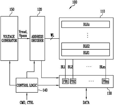
1. A method of operating a semiconductor memory device detecting a threshold voltage distribution for memory cells included in a page selected from among a plurality of memory cells, wherein each of the plurality of memory cells stores N bit of data, the method comprising:
selecting a target state, in which the threshold voltage distribution is to be detected, from among an erase state and first to (2N-1)-th program states, wherein N is a natural number;
determining a plurality of read voltages for dividing a voltage range in which a threshold voltage of the selected target state is distributed; and
performing a plurality of sensing operations using the plurality of read voltages on the selected page,
wherein masking to the target state is applied in each of the plurality of sensing operations.
|