| CPC G11C 16/10 (2013.01) [G11C 16/0483 (2013.01); G11C 16/24 (2013.01); G11C 16/3459 (2013.01); G11C 11/56 (2013.01)] | 20 Claims |
|
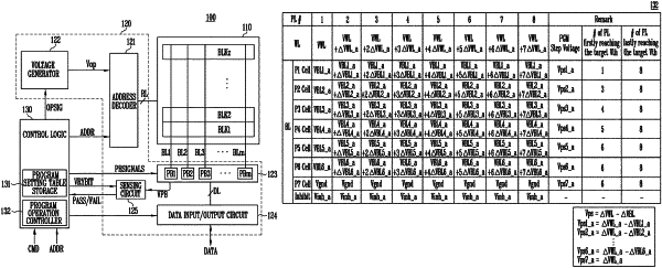
1. A memory device comprising:
a plurality of memory cells;
a peripheral circuit configured to perform an incremental step pulse program (ISPP) on a selected memory cell among the plurality of memory cells to a target program state among a plurality of program states; and
control logic configured to store a program setting table on bit line step voltages corresponding to the plurality of program states, respectively, and control the peripheral circuit to perform the ISPP using a bit line voltage set based on the target program state and the program setting table,
wherein the bit line step voltages have different values from each other according to corresponding program states, respectively, in the program setting table.
|