| CPC G11C 16/08 (2013.01) [G11C 16/30 (2013.01)] | 15 Claims |
|
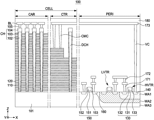
1. A semiconductor device comprising:
a peripheral circuit region including circuit elements on a substrate, the circuit elements of a page buffer and a row decoder; and
a cell region including gate electrode layers, stacked in a first direction, perpendicular to an upper surface of the substrate, and connected to the row decoder, and channel structures extending in the first direction to penetrate through the gate electrode layers and to be connected to the page buffer,
wherein the row decoder includes high-voltage elements, operating at a first power supply voltage, and low-voltage elements operating at a second power supply voltage, lower than the first power supply voltage,
at least one first high-voltage element, among the high-voltage elements, is in a first well region doped with impurities having a first conductivity-type, and
at least one of the low-voltage elements is in a second well region surrounding the first well region and doped with impurities having a second conductivity-type, different from the first conductivity-type.
|