| CPC G11C 13/0069 (2013.01) [G06N 3/04 (2013.01); G11C 13/004 (2013.01); H10B 63/34 (2023.02); H10N 70/8833 (2023.02)] | 20 Claims |
|
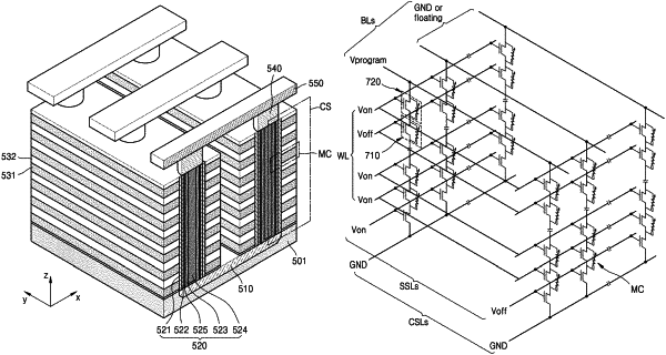
1. A nonvolatile memory device comprising:
a plurality of memory cell strings that each include
a semiconductor layer extending in a first direction and having a first surface opposite a second surface,
a plurality of gates and a plurality of insulators extending in a second direction perpendicular to the first direction, the plurality of gates and the plurality of insulators being alternately arranged in the first direction,
a gate insulating layer extending in the first direction between the plurality of gates and the first surface of the semiconductor layer and between the plurality of insulators and the first surface of the semiconductor layer, and
a dielectric film extending in the first direction on the second surface of the semiconductor layer, the dielectric film including a mixture of a material of the semiconductor layer and a transition metal oxide.
|