| CPC G11C 11/412 (2013.01) [G11C 11/419 (2013.01); H10B 10/125 (2023.02)] | 9 Claims |
|
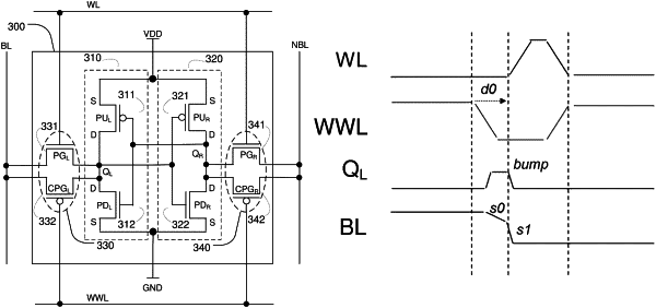
1. A memory cell, comprising:
a pair of cross-coupled inverters as a storage element, a first inverter in the pair of cross-coupled inverters having a first output at a first node, a second inverter in the pair of cross-coupled inverters having a second output at a second node;
a first complementary transmission gate including a first nMOS pass gate and a first pMOS pass gate, connected between the first node and a first bit line;
a second complementary transmission gate including a second nMOS pass gate and a second pMOS pass gate, connected between the second node and a second bit line;
a first word line connected to gate conductors of the first and second nMOS pass gates in the first and second complementary transmission gates; and
a second word line connected to gate conductors of the first and second pMOS pass gates in the first and second complementary transmission gates,
wherein a signal drop is triggered on the second word line to generate a first voltage drop on the first bit line,
wherein, after the signal drop is triggered on the second word line, a bump voltage is generated at the first node and then the bump voltage drops, and
wherein a signal rise is triggered on the first word line, after the bump voltage drops, to generate a second voltage drop on the first bit line.
|