| CPC G11C 11/4091 (2013.01) | 18 Claims |
|
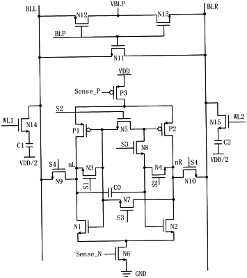
1. A sense amplifier, comprising:
an amplification module; and
an offset voltage storage unit, electrically connected to the amplification module;
wherein the amplification module comprises:
a first p-channel metal-oxide semiconductor (PMOS) transistor;
a second PMOS transistor, a source of the second PMOS transistor being connected to a source of the first PMOS transistor;
a first n-channel metal-oxide semiconductor (NMOS) transistor, a drain of the first NMOS transistor being connected to a drain of the first PMOS transistor and a first terminal of the offset voltage storage unit, and a gate of the first NMOS transistor being connected to a gate of the first PMOS transistor; and
a second NMOS transistor, a drain of the second NMOS transistor being connected to a drain of the second PMOS transistor, a source of the second NMOS transistor being connected to a source of the first NMOS transistor, and a gate of the second NMOS transistor being connected to a second terminal of the offset voltage storage unit;
wherein, in an offset cancellation stage of the sense amplifier, the first PMOS transistor and the second PMOS transistor are configured as a current mirror, and the first NMOS transistor and the second NMOS transistor are both configured by using a diode connection mode, to store an offset voltage of the amplification module in the offset voltage storage unit.
|