| CPC G11C 11/405 (2013.01) [H01L 27/1207 (2013.01); H01L 27/1225 (2013.01); H01L 27/1255 (2013.01); H01L 29/7869 (2013.01); H01L 29/78648 (2013.01); H03K 3/012 (2013.01); H10B 12/00 (2023.02)] | 8 Claims |
|
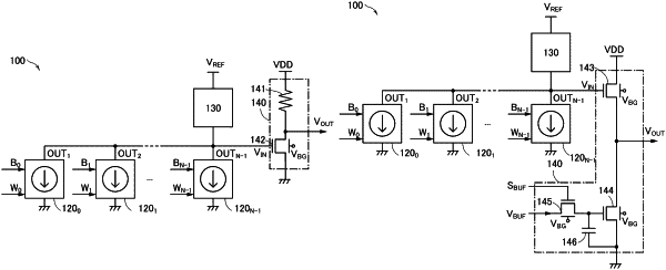
1. A semiconductor device comprising:
a plurality of constant current circuits each including a first transistor, a second transistor, and a third transistor,
wherein a gate of the first transistor is electrically connected to one of a source and a drain of the third transistor,
wherein a gate of the second transistor is electrically connected to a first wiring which transmits a digital signal,
wherein the other of the source and the drain of the third transistor is electrically connected to a second wiring which transmits an analog potential,
wherein a first current corresponding to the analog potential flows through the first transistor,
wherein the second transistor is configured to control the first current which flows through the first transistor, in response to the digital signal, and
wherein the first transistor, the second transistor, and the third transistor each include a semiconductor layer including an oxide semiconductor in a channel formation region.
|