| CPC G11C 11/4023 (2013.01) [G11C 11/4074 (2013.01); G11C 11/4097 (2013.01); H01L 27/0924 (2013.01); H10B 12/37 (2023.02)] | 20 Claims |
|
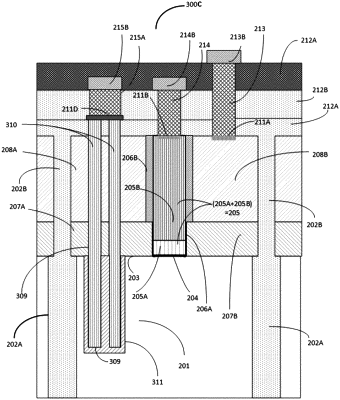
1. A dynamic random-access memory (DRAM) cell, comprising:
an epitaxially grown source having a doping of a second type, the epitaxially grown source over and in contact with a source region of a surface of a semiconductor substrate, the semiconductor substrate having a doping of a first type opposite to the second type, forming a junction at an interface between the source region of the surface of the semiconductor substrate and the epitaxially grown source;
an epitaxially grown drain having a doping of the second type, the epitaxially grown drain over and in contact with a drain region of the surface of the semiconductor substrate, the semiconductor substrate having a doping of the first type opposite to the second type, forming a junction at an interface between the drain region of the surface of the semiconductor substrate and the epitaxially grown drain;
a gate structure on the surface of the substrate, separating the source region and the drain region of the surface of the semiconductor substrate, the gate structure having a gate dielectric separating a conductive gate electrode from the surface of the semiconductor substrate;
a pass gate comprising the conductive gate electrode enabled to create a conductive channel in the semiconductor substrate under the gate dielectric, the conductive channel electrically connecting the epitaxially grown source over the source region and the epitaxially grown drain over the drain region when a gate voltage in excess of a threshold voltage of a pass transistor is applied to the conductive gate electrode;
a capacitor structurally integrated into the epitaxially grown source, the capacitor having a first terminal connected to the epitaxially grown source and a second terminal connected to a ground terminal or a fixed voltage terminal; and
a capacitor dielectric separating the first and second terminals of the capacitor;
wherein
when the pass transistor is turned on, the first terminal of the capacitor is electrically connected to a bit line connected to the epitaxially grown drain; and
when the pass transistor is turned off, the first terminal of the capacitor is isolated from the bit line connected to the epitaxially grown drain.
|