| CPC G11C 11/1675 (2013.01) [G11C 11/1655 (2013.01); G11C 11/1657 (2013.01); G11C 11/1673 (2013.01); G11C 11/1697 (2013.01)] | 19 Claims |
|
1. A memory device comprising:
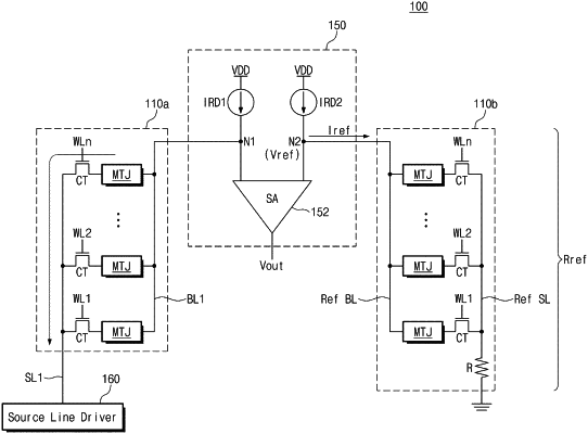
a memory cell array including a first region and a second region, the second region configured to store a value of a write voltage, the write voltage based on a value of a reference resistor for determining whether a programmed memory cell is in a parallel state or anti-parallel state, the value of the reference resistor determined by comparing a voltage drop across a first reference bit line in the first region with a voltage drop across a second reference bit line in the second region;
a voltage generator configured to generate a code value based on the value of the write voltage; and
a write driver configured to drive a write current based on the code value, the write current being a current for storing data in the first region.
|