| CPC G09G 3/3677 (2013.01) [G09G 3/3688 (2013.01); G09G 2340/0435 (2013.01)] | 14 Claims |
|
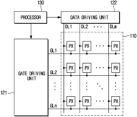
1. A method of controlling a display device, the method comprising:
outputting gate signals through a plurality of gate lines including a first gate line, a second gate line and a third gate line; and
applying, through a plurality of data lines, a data voltage to a plurality of pixels connected with a plurality of switching elements to which the gate signals were output,
wherein the outputting the gate signals comprises:
in a first mode, sequentially outputting gate signals to the plurality of gate lines one gate line at a time to process image data in a first driving frequency; and
in a second mode, outputting gate signals to the plurality of gate lines at least two gate lines at a time to process image data in a second driving frequency higher than the first driving frequency,
wherein, in the second mode,
respective ones of the gate signals output to the plurality of gate lines at least two gate lines at a time have output timings different from each other, and
outputting the gate signals to the plurality of gate lines at least two gate lines at a time includes:
outputting a first gate signal to a plurality of switching elements connected to the first gate line through the first gate line at a first timing,
outputting a second gate signal to a plurality of switching elements connected to the second gate line through the second gate line at a second timing, and
outputting a third gate signal to a plurality of switching elements connected to the third gate line through the third gate line at a third timing,
wherein a plurality of pixels connected with the second gate line are charged by a third value based on a first value by which a plurality of pixels connected to the first gate line are charged and a second value by which a plurality of pixels connected to the third gate line are charged, and wherein the third value is different from the first value and the second value.
|