| CPC G09G 3/3648 (2013.01) [G09G 3/20 (2013.01); G09G 3/3677 (2013.01); G09G 2300/0426 (2013.01); G09G 2310/0267 (2013.01); G09G 2310/0286 (2013.01); G09G 2320/043 (2013.01); G09G 2352/00 (2013.01); H03K 17/04 (2013.01)] | 7 Claims |
|
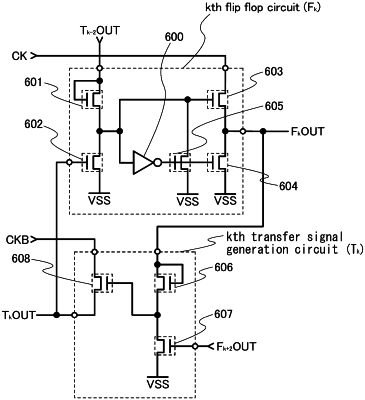
1. A semiconductor device comprising:
a first transistor, a second transistor, a third transistor, a fourth transistor, a fifth transistor, a sixth transistor, a seventh transistor, an eighth transistor, and a ninth transistor,
wherein one of a source and a drain of the first transistor is electrically connected to a first wiring,
wherein the other of the source and the drain of the first transistor is electrically connected to a second wiring,
wherein one of a source and a drain of the second transistor is electrically connected to the first wiring,
wherein the other of the source and the drain of the second transistor is electrically connected to a third wiring,
wherein one of a source and a drain of the third transistor is electrically connected to a gate of the first transistor,
wherein the other of the source and the drain of the third transistor is electrically connected to a fourth wiring,
wherein a gate of the third transistor is electrically connected to the fourth wiring,
wherein one of a source and a drain of the fourth transistor is electrically connected to the gate of the first transistor,
wherein a gate of the fourth transistor is electrically connected to a fifth wiring,
wherein one of a source and a drain of the fifth transistor is electrically connected to a gate of the second transistor,
wherein the other of the source and the drain of the fifth transistor is electrically connected to the third wiring,
wherein a gate of the fifth transistor is electrically connected to the gate of the first transistor,
wherein one of a source and a drain of the sixth transistor is electrically connected to the fifth wiring,
wherein the other of the source and the drain of the sixth transistor is electrically connected to a sixth wiring,
wherein one of a source and a drain of the seventh transistor is electrically connected to the fifth wiring,
wherein the other of the source and the drain of the seventh transistor is electrically connected to the third wiring,
wherein a gate of the seventh transistor is electrically connected to a seventh wiring,
wherein one of a source and a drain of the eighth transistor is electrically connected to a gate of the sixth transistor,
wherein a gate of the eighth transistor is electrically connected to the first wiring,
wherein one of a source and a drain of the ninth transistor is electrically connected to the gate of the sixth transistor,
wherein the other of the source and the drain of the ninth transistor is electrically connected to the third wiring, and
wherein a gate of the ninth transistor is electrically connected to the seventh wiring.
|