| CPC G09G 3/3629 (2013.01) [G09G 3/3614 (2013.01); G09G 3/3677 (2013.01); G09G 3/3688 (2013.01); G09G 2300/0842 (2013.01); G09G 2310/0278 (2013.01); G09G 2310/0291 (2013.01); G09G 2330/021 (2013.01)] | 16 Claims |
|
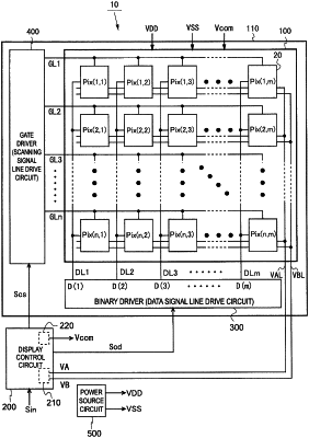
1. A display device that performs binary display using a pixel circuit having a memory function, the display device comprising:
a plurality of pixel circuits configured to form an image to be displayed;
a first power source line and a second power source line;
a first selection control line and a second selection control line; and
a selection control circuit configured to generate a first selection control signal and a second selection control signal to be applied to the first selection control line and the second selection control line, respectively,
wherein each of the plurality of pixel circuits includes
a display element including a pixel electrode and configured to be driven by a voltage for which a polarity is periodically inverted,
a pixel memory circuit including a first node and a second node, the first node being configured to hold one of a voltage of the first power source line and a voltage of the second power source line in accordance with a pixel corresponding to the pixel circuit of the image to be displayed, and the second node being configured to hold, of the voltage of the first power source line and the voltage of the second power source line, the voltage that is different from the voltage held at the first node, and
a voltage selection circuit configured to select a voltage to be applied to the pixel electrode from the voltage of the first node and the voltage of the second node,
the voltage selection circuit includes
a first selection transistor, as a switching element, including a first conduction terminal connected to the first node, a second conduction terminal connected to the pixel electrode, and a control terminal connected to the first selection control line, and
a second selection transistor, as a switching element, including a first conduction terminal connected to the second node, a second conduction terminal connected to the pixel electrode, and a control terminal connected to the second selection control line, and
the selection control circuit generates the first selection control signal and the second selection control signal to cause the first selection transistor and the second selection transistor to be turned on and off periodically in a mutually inverted manner.
|