| CPC G09G 3/3275 (2013.01) [G09G 3/3233 (2013.01); G09G 2300/0819 (2013.01); G09G 2300/0842 (2013.01); G09G 2310/0291 (2013.01); G09G 2310/08 (2013.01); G09G 2330/021 (2013.01); G09G 2330/028 (2013.01)] | 20 Claims |
|
1. A display device comprising:
a display panel including a plurality of pixels;
a data driver configured to output data signals to the plurality of pixels during a writing frame and configured to output a bias voltage to the plurality of pixels during a holding frame; and
a scan driver configured to output scan signals to the plurality of pixels,
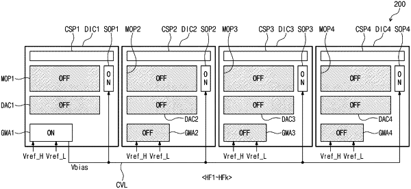
wherein the data driver includes a plurality of driving chips,
wherein each of the plurality of driving chips includes:
a gamma voltage generator configured to output a gamma voltage;
a data converter configured to convert image data into corresponding data signals of the data signals based on the gamma voltage;
a main output part configured to output the corresponding data signals during the writing frame; and
a sub-output part configured to output the bias voltage during the holding frame, and
wherein the gamma voltage generator of a selected driving chip among the plurality of driving chips is electrically connected to a plurality of sub-output parts which is disposed in the plurality of driving chips, respectively.
|